From Simulation to Precision Manufacturing
Each socket is engineered before it is built — FEA stress, signal integrity, and thermal validation up front, then precision-manufactured for high-speed, high-density test across GPU, AI, communication, MEMS, and automotive semiconductors.
- 80 GHz Coax — X Series with measured S21/S11 data
- 0.13 mm Pitch — wafer-level down to 130 μm
- 300K Cycles — Zalloy probes for extended life
- 24h Response — engineering review within one business day
No obligation · NDA available · Engineering team in Suzhou & Kansas
- ISO 9001 / IATF 16949 / ISO 14001 / 13485 Certified
- Serving Customers in 16 Countries
- In-house FEA & Signal Integrity Simulation
- Zalloy Proprietary Probe Alloy
Quick Match
Find the Right Socket in 60 Seconds
Tell us what you're testing — get a platform recommendation from our engineering team.
Find the Right Socket in 60 Seconds
Tell us what you're testing — get a platform recommendation.
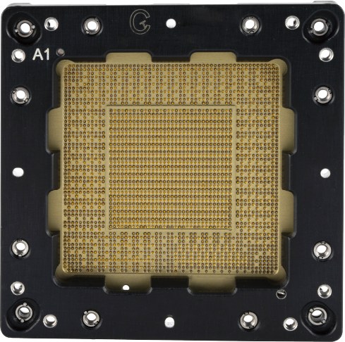
Coaxial Structure, Measured to 80 GHz
S21 / S11 verified on the network analyzer — not simulated only.
A true coaxial structure in every probe — inner signal conductor, dielectric layer, and outer ground shield — overcomes the bandwidth ceiling of composite plastic sockets for GPU, AI accelerators, 112G/224G SerDes, and millimeter-wave testing.
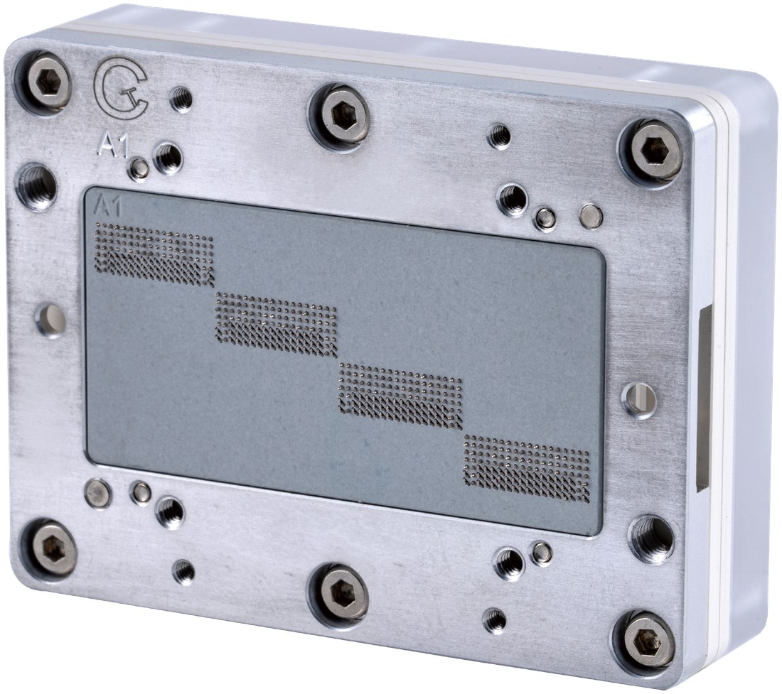
Down to 130 μm at Wafer Level
KGD probing with replaceable cartridge modules.
From 0.13 mm wafer-level pitch to 1.00 mm area-array packages, Zalloy probes maintain stable contact across hundreds of thousands of insertions — with minimal PCB deflection, multi-site support, and optional Kelvin testing for high-power dies.
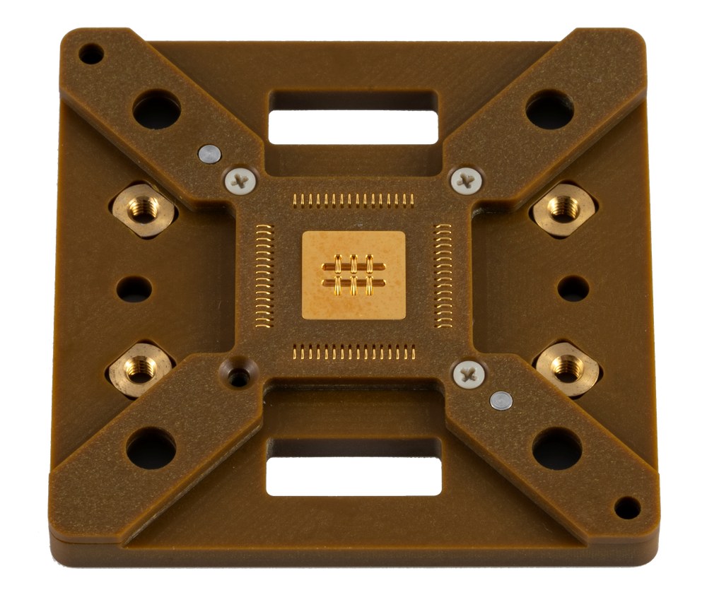
300,000+ Contact Cycles
In-house Zalloy alloy, validated by 100% in-line inspection.
Our proprietary Zalloy material extends contact life, withstands aggressive cleaning cycles, and holds stable contact resistance over hundreds of thousands of insertions — reducing consumable cost per test in high-volume production.
Platform Comparison
Compare All Six Socket Platforms
Key specs at a glance — six socket platforms compared.
| Parameter | Area Array | Z Series | X Series (Coax) | Family | MEMS/Sensor | Wafer Level |
|---|---|---|---|---|---|---|
| Pitch Range | 0.25–1.00 mm | ≥0.30 mm | ≥0.35 mm | 0.25–1.00 mm | Per application | 130–500 μm |
| Max Bandwidth | — | 15–40 GHz | 45–80 GHz | — | — | >5 GHz RF |
| Max Current | ≥3–5A | ≥3–5A | 3.0A | Per config | Per config | Per config |
| Contact Cycles | 250K+ | 250–300K | 300K | Per config | Per config | Zalloy, extended |
| Contact Resistance | Low | ≤30 mΩ | ≤60 mΩ | Per config | Per config | Per config |
| Temp Range | Per config | -40~155°C | -40~120°C | Per config | Environmental sim | Per config |
| Package Size | Per config | Per config | Per config | 3–50 mm | Circ./Rect. | Wafer |
| Key Strength | High pin count | Balanced HF | Ultra-high freq | Modular | Env. simulation | Ultra-fine pitch |
The UIGREEN Difference
Why Choose UIGREEN
Three capabilities that set our sockets apart from commodity alternatives.
Zalloy Proprietary Probe Alloy
Our in-house Zalloy material extends contact life, withstands aggressive cleaning cycles, and maintains stable contact resistance over hundreds of thousands of insertions — reducing consumable cost per test.
Simulation Before Tooling
Every custom socket starts with FEA stress analysis, signal integrity simulation, and thermal/CFD modeling. We validate contact force, impedance, and heat dissipation virtually — before cutting a single part.
In-House Full-Process Manufacturing
From deep draw and precision machining to micro laser drilling, micro plating, and insert molding — we control the full process in-house, enabling rapid iteration and consistent quality at scale.
Applications
What We Test
Three core domains across the semiconductor value chain.
Semiconductor Package Test
Final test and system-level test for GPUs, CPUs, AI accelerators, communication chips, and automotive semiconductors. High-frequency, high-current, and high-pin-count coverage.
MEMS: Sensor & Microphone
Environmental-simulation test for MEMS sensors and microphones. Temperature, air pressure, and acoustic condition emulation with seamless, air-pressure-loaded socket designs.
Fine-Pitch PCB / Flex PCB Test
High-density interconnect testing for fine-pitch rigid and flexible PCBs. Wafer-level and probe-card-level solutions with minimal deflection and multi-site support.
Capabilities
From Simulation to Precision Manufacturing
In-house engineering and manufacturing across the full socket development lifecycle.
Engineering
- RF & System Modeling
- CAD/CAM & Solid Modeling
- Reliability Analysis
- Finite Element Analysis (FEA)
- Signal Integrity Simulation
- Thermal Analysis & CFD
Manufacturing
- Deep Draw Capability
- Precision Machining
- Validation Testing
- Contact Assembly
- Micro Laser Drilling
- Micro Plating & Insert Molding